The racetrack logic technology enables the development of solid-state memories in which it is possible to elaborate the data stored in it. This important feature avoid the needs of moving data continously between the CPU and the main memory.

This computing paradigm reduces the power dissipation, extending the battery life of our PCs or smartphones.

Moreover, the highly parallel structure of the racetrack logic technology makes it suitable for graphic and AI tasks.

Patent Status

PENDING

Patent Priority

102019000013542

Priority Date

31/07/2019

License

INTERNATIONAL

Market

The market revenues related to non-volatile memories was about $600M in 2020 and it is expected to reach $3.3B in 2026.

The growth rate of the non-volatile memory market shows a CAGR of 110% from 2020 to 2026.

The serviceable addressable market is the one related to non-volatile memories and in particular the one integrated in microcontrollers (MCU), System on Chip (SoC) and ASIC. This market holds about 100% of the currently non-volatile memories.

Problem

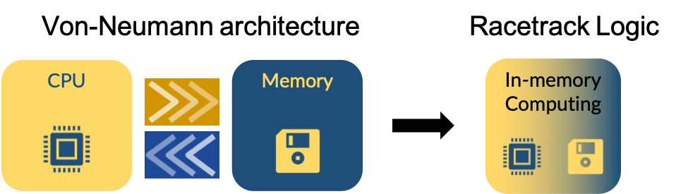
Currently, the computing paradigm adopted in the PCs and Smartphones is based on the Von-Neumann architecture, where a processing unit (CPU) and the memory are present. This organization requires a continous exchange of data between the processor and the memory in order to perform elaboration and dissipates a lot of power.

The technology proposed, the racetrack logic, is a non-volatile memory with computing capabilities. The computation is performed directly on the stored data. The proposed device can implement logic functions that cannot be integrated in standard memories.

Moreover, the computation is executed in parallel over the whole array in a single clock cycle, without the need of external circuitry.

Having the possibility to perform the elaboration locally, within the memory, the data transfer between the CPU and the main memory is drastically reduced, especially for data intensive applications. The data transfer is energetically expensive and must be reduced in order to increase the battery life of portable devices.

The racetrack logic technology can have a strong impact on all portable electronic devices like IoT nodes, tablets, PC or smartphones. Indeed, the aim of device manufacturers is not only to achieve higher performance, but also to increase the battery life of their products.

Current Technology Limits

Existing solutions on the market do not offer a real solution to the problem, they do not allow the execution of logic functions directly within the memory cell. In the current Von-Neumann paradigm, the data to be processed are transported outside the memory, processed and stored again within the memory. In the literature, some solutions are proposed, defined as “near memory”. Here, some specific functions are performed externally to the processor to reduce the latency given by the data transfer from the memory. However, this solution solves just partially the problem under analysis, in fact, while optimizing some specific processes, the classic paradigm remains unchanged. Some well-known smartphone manufacturers are currently investing huge resources in researching new architectures aiming to improve the interaction between CPU and memories by using classic CMOS technology. Recently, modern architectural designs shows the integration of  CPU and GPU with a high-performance shared memory.

The solution proposed with racetrack memories represents a further advance in the search for effective solutions, based on a technology intrinsically endowed with unique physical characteristics, capable of integrating logic and memory functions, which the CMOS currently used cannot achieve.

Killer Application

  • January 2022: development of a prototype that demonstrates the implementation of the logic functions within the memory.
  • January 2023: development of a 3D fabrication process to increase the efficiency of the device and increase the data parallesim.

Our Technology and Solution

The realization of the racetrack memories is based on a multilayer stack of CoFeB and MgO. After being deposited through a deposition process, it is structured to obtain the magnetic strips necessary to store data.

By means of electrical contacts, suitably defined at the ends of the strips of magnetic material, it is possible to move data by exploiting a current that passes through the material.

Advantages

The main advantages of the proposed invention are:

  • The same device can work both as a memory element and as a calculation element by reducing the latency introduced by the of Von-Neumann paradigm
  • The high density of the device enables the achievement of high levels of parallelism, allowing the data stored within the memory to be processed simultaneously
  • Each memory cell is independent and can perform multiple logic functions, it can be reprogrammed run-time during the execution of a program
  • It is possible to create three-dimensional calculation structures to increase the density and parallelism of the processor

Roadmap

The € 50k loan, granted by the Compagnia di San Paolo and Liftt in 2021, made it possible to accelerate the development of the prototype by validating the individual elements of the manufacturing process.

The roadmap for the realisation of a complete prototype requires to:

  1. Validate the 3D manufacturing process started during the financed activities (just ended)
  2. Experimentally create a device with multiple memory cells. In this prototype, MTJ devices have been adopted for writing and TMR devices were adopted for reading data
  3. Get in touch with potential investors in the semiconductor industry interested in obtaining the patent under license We are currently in contact with a research laboratory located in Munich which gives us free access to its laboratories and in particular to the “clean room”. It is also required to cover the cost of personnel (PhD or researcher) who will have to carry out the experiments as well as the cost of consumables.
Review the Technology
TRL 1
TRL 2
TRL 3
TRL 4
TRL 5
TRL 6
TRL 7
TRL 8
TRL 9

TRL

Team

Menu